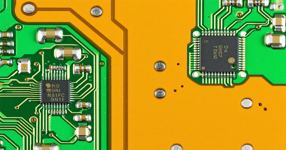
PCB solder joint inspection has more physical complexity per square inch than almost any other end-of-line inspection task. You are looking at joints that are 0.5mm to 1.5mm in diameter, with a reflective meniscus shape that changes with joint quality, on a board that may carry 400–2,000 joints in a single field of view. Getting the setup wrong means high false rejects on acceptable joints or missed detects on bridging and cold solder. Getting it right requires deliberate choices on lighting geometry, camera selection, working distance, and training data composition.
Lighting Geometry: The Decision That Everything Else Depends On
Solder joint quality is encoded in the joint's surface geometry. A good reflow joint on an SMD component has a concave meniscus with smooth, shiny surface — indicative of proper wetting and adequate solder volume. A cold joint has a dull, grainy surface with a convex or irregular meniscus — indicating insufficient reflow temperature or contaminated pad. A solder bridge connects two adjacent pads and appears as an elongated high-intensity blob between them.
These visual signatures depend entirely on how light reaches the joint surface. Three lighting configurations are used in PCB solder inspection:
Coaxial illumination directs light along the optical axis of the camera lens via a beam splitter. The camera sees the direct reflection of the light source from specular surfaces. On a properly wetted solder joint, the top of the meniscus reflects strongly toward the camera — it appears as a bright spot in the center of the joint. A cold joint or poorly wetted joint scatters light diffusely and appears dull. Coaxial illumination is the primary choice for joint quality detection because it directly encodes the wetting signature in pixel intensity.
Angled ring illumination at 45–70° from the optical axis creates side-lighting that reveals joint geometry through shadow patterns. Ring lighting at steep angles shows the joint outline and reveals bridging artifacts between adjacent pins. A solder bridge under 45° ring lighting creates a continuous bright line between pin pads — detectable as an over-length blob in classical blob analysis or a high-confidence bridge-class output from a CNN.
Darkfield illumination at very shallow angles (10–20° from the board plane) reveals surface texture and contamination. Solder paste residue, flux residue, and board surface contamination appear as bright regions under darkfield. Less common for joint quality inspection, more useful for post-soldering cleanliness checks on medical device or aerospace boards.
For a general-purpose PCB end-of-line inspection station covering joint quality, bridging, tombstoning, and component presence: use coaxial illumination as the primary light source, combined with a programmable ring light for on-demand angled exposures. Most deployments capture two images per board position — one under coaxial, one under 45° ring — and run joint classification on the coaxial image with bridge detection on the ring image.
Camera Selection: Area Scan vs Line Scan for PCB
Area scan cameras capture the entire field of view in a single exposure. They are the standard choice for board-level PCB inspection where the board is stationary during imaging. A 5MP area scan camera (e.g., Basler ace2 series) at 500mm working distance with an appropriate macro lens gives a field of view covering a 60mm × 45mm board region at 12µm/pixel resolution — sufficient to resolve a 0.5mm solder joint across approximately 40 pixels, giving good classifier input quality.
For a full-board inspection at 200mm × 150mm board size, you need either a larger sensor (20MP+) or a multi-station inspection with multiple camera heads. A 20MP area scan camera at the same working distance gives approximately 6µm/pixel, resolving the full board in a single shot with adequate joint detail. Inference time increases with image size — budget 80–120ms for a 20MP image through a joint classifier on a mid-tier GPU.
Line scan cameras scan the board one pixel-row at a time as it moves under the camera on a conveyor. Line scan is common in high-throughput electronics final assembly lines where boards never stop — they travel continuously at 0.3–0.8m/s. Line scan at 4096 pixels wide and 30kHz line rate captures a full 200mm-wide board in under 700ms of transit time, faster than any area scan stop-and-shoot approach at comparable resolution. The tradeoff: line scan requires precise conveyor speed synchronization via encoder input, and coaxial illumination for line scan is more complex (requires a line-format beam splitter or co-axially illuminated line laser).
For most contract manufacturing electronics final assembly lines running at cycle times above 4 seconds per board, area scan is simpler to deploy and maintain. Line scan is worth the additional complexity when boards run continuously at speeds above 0.5m/s or when the line cannot accommodate a stop-and-shoot dwell station.
Working Distance and Depth of Field
PCB solder joint inspection has a depth of field challenge: through-hole component leads, tall electrolytic capacitors, and connectors create a depth range of 15–30mm across the board surface. A lens set for optimal focus on the board surface goes out of focus at the top of a 25mm capacitor. For a joint classifier trained on board-surface-height images, the defocused appearance of a tall component's lead joint can trigger false rejects — the CNN has never seen a properly soldered joint that looks blurry.
Practical approaches:
- Zone-based focus: Segment the board into inspection zones by component height. Configure separate camera positions (or a motorized focus stage) for tall-component zones and SMD zones.
- Large depth of field optics: Telecentric lenses maintain focus over a larger depth range than standard lenses at equivalent magnification. More expensive, but eliminates zone-switching for moderate-height variation (<10mm).
- Accept height-variant training images: Include images of properly soldered tall components at normal operating focus in your training set. A CNN trained to recognize that a mildly defocused through-hole joint is still a good joint (because it is on a tall component at the camera's nominal working distance) will not false-reject those joints.
Training Data: How Many Images You Actually Need
This is the question that comes up in every electronics contract manufacturer pre-deployment conversation, and the honest answer is: fewer than you think, if collected correctly, and more than you want, if collected without a plan.
For a joint quality classifier distinguishing good joints from cold, insufficient, and bridged defect classes:
- Minimum viable training set: 300 good-joint images, 80–100 images per defect class. Total: ~600 images for a 3-class defect model. At this volume, a fine-tuned EfficientNet-B2 reaches 91–93% accuracy on a held-out validation set. Sufficient for initial deployment; expect continued improvement as production images are added to the training set over the first 4–6 weeks.
- Production-quality training set: 1,000+ good-joint images spanning multiple production batches (to capture solder paste lot variation), 200–300 images per defect class. At this volume, accuracy typically reaches 96–98% with false reject rate under 0.5% on production boards.
- Defect-scarce situation: Electronics contract manufacturers launching a new board design often have zero defect examples before production starts. PatchCore anomaly detection initialized on 400 good-joint images can start detecting significant deviations (bridges, missing solder, tombstones) with an AUC of ~0.88–0.92 before any labeled defect data is collected. It is not as accurate as a trained classifier at production-quality volume, but it is deployable on day one and improves passively as production runs.
We're not saying you need a large defect archive before you can deploy — that framing keeps plants running manual inspection for months while waiting for "enough data." The right approach is to deploy anomaly detection first, capture and label rejects as they occur, and migrate to a trained multi-class classifier once defect sample counts pass threshold.
IPC-A-610 Acceptability Criteria: Translating Standards into Classifier Labels
IPC-A-610 (Acceptability of Electronic Assemblies) defines three classes of acceptability for solder joints: Class 1 (general electronics), Class 2 (dedicated service electronics), Class 3 (high-reliability, including aerospace and medical). Each class has specific criteria for acceptable meniscus geometry, solder fill percentage for through-hole joints, and bridging tolerance.
When labeling training images, you need to label against the IPC-A-610 class relevant to your production — not against a generic "good/bad" binary. A joint that is acceptable per IPC Class 1 criteria may be a Class 2 reject. A training set labeled by a technician who does not know the target IPC class will produce a classifier with miscalibrated decision boundaries.
Practical recommendation: have your process engineer or IPC-CIS (Certified IPC Specialist) review a 200-image sample of your training labels before model training begins. Relabeling disagreements on 10–15% of images is common on first pass. That upfront 4-hour review saves 3 weeks of troubleshooting miscalibrated reject decisions after deployment.
For details on how Eolvision handles multi-class joint inspection across SMD and through-hole component types, including integration with MES for board-level traceability, see the electronics inspection page and the how it works overview.